受託研究および講演依頼受付中
日本製scatterometry装置製作にご協力ください。
光のマクスウェル解析は、アメリカに立ち遅れています。
LSIの技術は、2020年まで道筋(roadmap)が出来ています。
白崎教授は、米国SPIEに毎年(7年目)論文発表をして、注目されています。
また、玉川大学初代ソーラーカー「スーパーゲンボウ」の電装責任者として、
ソーラーセルをドイツから直輸入してモジュール作成、モーター、バッテリーの電装設計を行いました。
さらに、テーパ導波管やテーパ形マイクロストリップ線路の小型化設計理論は、実用化されています。
![]()
![]() Scatterometryについての詳細はこちらをご覧下さい。
Scatterometryについての詳細はこちらをご覧下さい。
次世代半導体集積回路リソグラフィ工程のscatterometry検査装置開発
白崎博公教授
[内容]
光波を用いたScatterometry(光波散乱計測)は、白崎教授の長年の研究によって世界でも最先端のノウハウを蓄積してきました。この技術を活用して、世界に先駆けて光波による3次元断面形状計測装置の製作を行い、先端分野における新技術開発のために貢献します。
もう少し詳しく ( Scatterometryについての詳細はこちらをご覧下さい。 )
ムーアの法則は、「LSIに集積可能なトランジスタの数は、約1.5年で2倍に増える」という技術開発スピードに関する経験則です。半導体のための2002年のインターナショナル・テクノロジー・ロードマップによれば、2004年に90ナノメートル、2010年に45ナノメートルの線幅計測が必要となります。さらに集積回路製作では、ウェハーサイズの大口径化による面内ばらつきの増加や、新材料の適用による不良要因の増加による非生産ウェハーを減らすことが重要です。しかし線幅が、光の波長の数分の一になる場合には、顕微鏡で検査する事はもはや出来ません。この断面形状測定を非破壊非接触で行う方法として、光波を用いたScatterometry(光波散乱計測)があります。scatterometryの基本は、光波長帯域における反射光のライン&スペース繰り返しパターン形状依存特性を数値解析より求め、実測値との比較よりパターン形状を求める方法です。
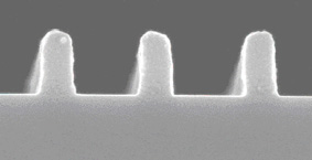 半導体トレンチの形状が、LSIの性能に影響してきます。
○平成9年度~平成12年度科学研究費補助金[基盤研究(C)(2)]
「干渉分光データのウェーブレット解析による半導体トレンチ形状測定」
(課題番号09650055)
○Scatteromtry 関連主要論文(他に電磁波導波関連論文多数あり)
(1)白崎博公、"斜め入射を考慮したFDTD法による次世代半導体線路幅形状のscatterometry計測"、
玉川大学工学部紀要, 39, pp.1-9 (2003-3-31).
(2)H. Shirasaki,"Arbitrary 3D linewidth forms measurement simulations
for the next-generation semiconductor circuits by scatterometry using the
FDTD method",SPIE's 18th annual symposium on microlithography.5375-170(2004-2-23)
(3)H. Shirasaki, et al,"Linewidth measurement simulations for semiconductor circuits by scatterometry using the FDTD and the time shortening calculation method", SPIE's 18th annual symposium on microlithography, 5375-169(2004-2-23)
(4)H. Shirasaki, et al, "Resist and Silicon Trench Array Linewidth
Measurement Simulations for the Next-Generation Semiconductor Circuits
by Optical Scattering Properties Using the FDTD Method", Proc. of
SPIE, Metrology, Inspection, and Process Control for Microlithography XVII,
5038 pp.748-756 (2003)
(5)白﨑博公、"FDTD法によるレジストとシリコン周期溝からの光波散乱特性解析"、玉川大学工学部紀要, 38, pp. 5-13 (2003-3-31).
(6)Hirokimi Shirasaki, "Shape Measurement Simulation for the Silicon
Trench by Scattering Properties and Continuous Wavelet Analysis Properties
with Interference Spectroscopy," 27th General Assembly of the International
Union of Radio Science, URSI 2002, B2-P-14 (2002).
(7)白﨑博公、"FDTD法による半導体周期溝からの光波散乱特性"、玉川大学工学部紀要, 37, pp.33-40 (2002-3-31).
(8)H.Shirasaki, "Shape Measurement Simulation for the Silicon Trench
Array by Scattering Properties and Continuous Wavelet Analysis with Interference
Spectroscopy,"Proc. of SPIE, Metrology, inspection, and process control
for microlithography XVI, vol.4689, pp.688-695 (2002-3).
(9)H.Shirasaki :"The depth measurement simulation for the dielectric
trench by continuous wavelet analysis with interference spectroscopy,"The
international conference on signal processing applications and technology,
ICSPAT '2000,pp.1-5(2000-10-19).
(10)H.Shirasaki :"Depth measurement simulation of dielectric trench
by FFT processing of interference spectroscopy,"The international
conference on signal processing applications and technology, ICSPAT '99,(1999-11-3).--at
Orange country convention center, Orland, Florida, USA.
(11)H. Shirasaki,"Depth and Width Measurement Simulation of Semiconductor
Trench by Optical Wave Irradiation", IEEE Transactions on Magnetics,
Vol.33,No.2,pp.1428-1431(1997-03-31).
![]()